ASIC Flows
Introduction
Very Large Scale Integration is a method to create an IC (Integrated Circuit) made up of millions or billions of transistors on a single chip. The first-ever integrated circuit was built by Jack Kilby in 1958 at Texas Instruments. The latest Intel 8 cores 11th generation processor (in 2021) has approximately 6 billion transistors. Isn’t it a revolutionary and amazing process to fit millions/ billions of transistors in a single chip? Also, most of the engineering work revolves around balancing out equations within performance, power consumption, area, price, etc.
There is phenomenal growth happening in the VLSI industry due to rapid advancement in IC technology, manufacturing process improvement, etc. This growth will continue further to supply the demands for consumer electronics, electric vehicles, communication system design, medical instruments, IoT, storage, artificial intelligence, etc.
What is ASIC in VLSI?
As the name ASIC (Application-specific integrated circuit) suggests, it is dedicated to perform tasks for a particular application. For example memory blocks like ROM, RAM, EEPROM, flash memory, chips used in washing machines, cellphones, televisions, etc.
It is one time manufactured and typically fabricated using MOS (Metal Oxide Semiconductor) technology.
It is important to understand ASIC flow for VLSI engineers. Basically, it is broadly classified into two parts front end and back end.
- The front end includes defining architecture, RTL design, and functional verification.
- The back end includes synthesis, STA, physical design, gate-level simulations, fabrication, post-silicon validation, DFT, etc.
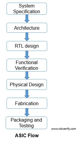
Let’s dive deeper into ASIC flow and see what exactly happens at each stage.
- ASIC Design Flow
- ASIC Verification Flow
- ASIC Physical Design Flow (Backend Flow) and Post Silicon Flow