ASIC Physical Design Flow
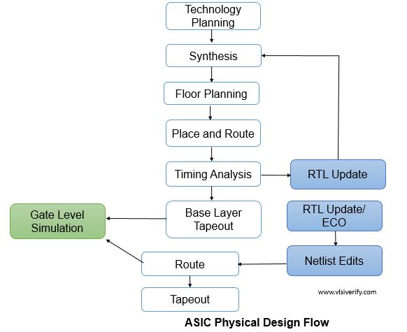
Technology Planning
Technology planning is an important step in the physical design flow. The technology libraries are provided by foundries that have information about the type of silicon wafer, standard cells, DRC(Design Rule Check), etc.
Synthesis
The synthesis process does conversion from synthesizable RTL code (higher level of abstraction) into gate-level netlist(lower level abstraction) of specific technology. In this phase, logic optimization, DFT logic insertion, logic equivalence between RTL and gate-level netlist is maintained.
Floorplanning
The floorplanning involves planning the placement of various modules on a chip and net routing in order to reduce congestion, and noise issues. It is one of the most important steps in backend or physical design flow that directly affects chip power consumption, timing, and reliability. For better floorplanning, you should have design and its data flow understanding, IO interactions within blocks, and outside blocks like analog IPs.
Place and Route
Actual standard cell placement in a chip boundary considering optimal consideration taken during floorplanning. The placement efforts are done by the PnR tool with minimal congestion, best timing, and preferences given by the user.
Timing Analysis
Static Timing Analysis (STA) checks for all possible paths in the design for any timing violations. Set up and hold timing violation is being checked as part of static timing analysis. STA is much faster as compared to dynamic timing analysis which is used to validate full design behavior for a given input vector stimulus because as the number of stimulus vectors increases, simulation time also increases in dynamic timing analysis. In brief, DTA checks for functionality, and STA checks for timing.
Gate level Simulation (GLS)
RTL simulation is done as functional verification whereas GLS is run when gate-level netlist is ready i.e. RTL simulation is pre-synthesis and GLS is post-synthesis. Usually, GLS is run with unit delay mode and full delay mode. The standard delay file (SDF) contains timing information that is considered as delay mode. Though GLS verification is a dead slow process, it provides benefits like reset and initialization flow check, asynchronous design timing check, X propagation in RTL, etc.
Tapeout
Once physical design verification is done, final design files are sent to the foundry for chip fabrication.
ASIC Post Silicon Flow
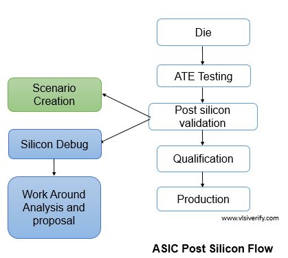
As a part of post-silicon flow, once the chip/die is ready after fabrication, it is once again tested in a real-time environment before it dispatches to the market. Automatic Test Equipment (ATE) is a device that sends automatic test pattern generation (ATPG) to the device under test (DUT). Thus, post-silicon validation checks for its correctness and performance. ATE testing is much faster as compared to RTL simulation. Once the chip is qualified as per testing norms, it is sent for production to deliver the market need.
ASIC Flows