Tutorials
Protocols
Learn More
Job roles in VLSI industry
The VLSI industry has much more to offer and it needs engineers like you right from the beginning architecture phase till the final product comes out.
In this article, you will understand all the different job roles available in the VLSI industry. Depending on your interests and educational background, you can choose to opt for a specific job role. To develop a product, in our case, it is a chip we first have to think of its functionality and its application where it will be used, based on which ASIC (Application Specific Integrated Circuit) will be manufactured.
The job roles are broadly classified into two parts:
- Front End
- Back End
Let’s understand the process of developing a chip along with job roles.

Job Market Growth in the VLSI Industry
As per the Ministry of Electronics and Information Technology, the demand for semiconductors in India is projected to surge to $70-$80 billion by 2026, driven by the rising appetite for digital devices and electronic products. Several prominent global semiconductor companies are increasing their presence in India by establishing research and development centres. This strategic move is motivated by India’s rising status as a technology innovation hub and its wealth of skilled talent in electronics and semiconductor engineering. Additionally, the country’s expanding middle class and growing demand for electronic devices and semiconductor components have made India an enticing market for these companies. The Indian government’s pro-industry initiatives and incentives further bolster this trend, fostering partnerships and investments that are poised to drive innovation, job creation, and technological advancements within the semiconductor sector, solidifying India’s position in the global semiconductor industry.
Front End Roles
A front-end role in VLSI encompasses responsibilities concentrated on the initial phases of integrated circuit design. Front-end VLSI engineers specialize in the conceptual and logical facets of chip design, utilizing hardware description languages (HDLs) and diverse design tools. Key aspects of this role involve digital and analog design, RTL design, design verification, etc
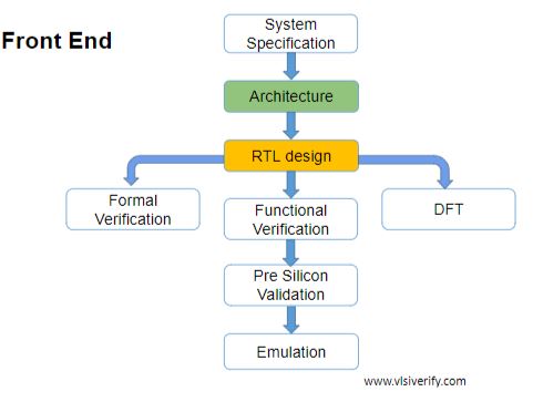
System Specification
At first, based on market trends and future requirements what has to be designed is being analyzed and captured as system specifications.
Architecture
As per system specifications, all features that need to be implemented in hardware and firmware/software are decided in this phase. An architectural team decides the data and control flows and can have different approaches to implement the hardware blocks and offload some work to the firmware. An optimized approach is selected considering various trade-offs like clock frequency, speed, power consumption, firmware execution time, etc. This is a very important step and a highly experienced group of team decides design architecture. It is difficult to get a role in an architect team during the initial phase of a career, but sometimes there is a requirement for modeling to illustrate or perform initial analysis that can help architects to decide design flows for which they may hire mid-senior level engineers.
RTL design
An RTL (Register-Transfer Level) designer plays a vital role in digital hardware design, responsible for translating high-level system requirements into detailed hardware descriptions. They craft RTL code, defining how data is transferred between registers and operations are performed, ensuring both functionality and efficiency. RTL designers optimize designs for performance, power consumption, and area utilization while collaborating with various teams to validate and refine designs through simulation and formal verification. Their work ensures that complex digital systems, from microprocessors to custom integrated circuits, meet their intended functionality and performance goals.
DFT
Design for Testability (DFT) testing is primarily done in the front-end phase of VLSI design. It is an integral part of the design process that focuses on making the chip or integrated circuit (IC) easier to test for manufacturing defects and ensuring efficient testing methods are available. DFT techniques and features are integrated into the chip’s design during the front-end engineering phase, which includes tasks such as RTL (Register-Transfer Level) design, logic synthesis, and functional verification. These techniques include the insertion of scan chains, boundary scan (JTAG), built-in self-test (BIST) structures, and other mechanisms that facilitate comprehensive testing of the chip’s functionality.
Functional Verification
Verification engineers play a critical role in the functional verification process, where their primary objective is to uncover defects while ensuring the RTL design aligns with the design specifications. The verification journey begins with the creation of a verification plan, based on the design specifications. This comprehensive plan outlines the features to be tested and delineates the strategies and techniques for validating the Design Under Test (DUT), including activities such as scoreboard planning and its coding, writing assertions, and establishing functional coverage criteria. Verification engineers act as the guardians of design integrity and scrutinize every aspect to ensure the robustness and correctness of digital systems.
Formal verification
A FPGA pre-silicon validation engineer is responsible for meticulously testing and verifying Field-Programmable Gate Array (FPGA) designs before they are manufactured, ensuring they meet functional, timing, power, and compliance requirements. This role involves creating and executing validation plans, developing test benches, conducting simulations, and analyzing results to identify and resolve design issues. FPGA pre-silicon validation engineers collaborate closely with design teams, use industry-standard tools and methodologies, and maintain comprehensive documentation to ensure the integrity and reliability of FPGA-based solutions for various applications.
Pre-silicon Validation
Relevant internships, research projects, or personal projects related to VLSI design can greatly enhance a fresher’s resume and demonstrate practical skills.
Emulation
The emulation engineer’s primary responsibility is to use emulation platforms to simulate and validate the behaviour of complex electronic systems and integrated circuits (ICs) before they are manufactured. Emulation engineers also focus on optimizing design performance within the emulation environment, ensuring that the final product meets stringent functionality and performance criteria. Their work is essential for mitigating risks, accelerating development cycles, and ensuring the reliability of electronic systems in diverse applications.
Back End Roles
The back-end role is also an important semiconductor design process. Back-end engineers focus on transforming the logical design of integrated circuits into physical layouts that can be manufactured. They are responsible for tasks such as placement, routing, clock tree synthesis, power planning, and physical verification. Back-end engineers work to optimize chip size, minimize power consumption, and ensure signal integrity and manufacturability. Their role ensures that the designed chips meet performance and quality standards, addressing the physical constraints of semiconductor technology. Physical design engineers play an important role in physical chip development. Their core duties center on the conversion of a chip’s logical or RTL (Register-Transfer Level) design into a tangible physical layout ready for manufacturing. Some of the primary tasks and roles they commonly undertake include:
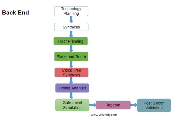
Technology planning
In the physical design process, foundries provide libraries containing vital details regarding silicon wafer types, standard cells, and design rule checks (DRC) which check whether the layout adheres to specific design rules and constraints provided by the semiconductor foundry or design team.
Synthesis
The synthesis process does conversion from synthesizable RTL code (higher level of abstraction) into gate-level netlist(lower level abstraction) of specific technology. In this phase, logic optimization, DFT logic insertion, and logic equivalence between RTL and gate-level netlist is maintained which is commonly known as LVS (Layout vs. Schematic)
Floorplanning
Physical design engineers determine the overall chip floorplan, deciding how to place different functional blocks, memory components, and other elements on the silicon die. This involves optimizing chip size, power distribution, and signal routing. Placement: They place individual standard cells, macros, and other components within the chip’s designated areas, considering factors such as signal timing, power, and area constraints.
Place and Route
Physical design engineers create the physical interconnections (wires and metal layers) between various components, ensuring efficient data flow while adhering to design rules and constraints.
Clock Tree Synthesis
They design and optimize the clock distribution network to ensure that clock signals are distributed evenly and without skew to all parts of the chip, addressing critical timing considerations. Power Planning and Analysis: Engineers work on power distribution strategies, minimizing power consumption while ensuring stable power delivery to all sections of the chip. They also perform power analysis to assess and manage power consumption.
Timing Analysis
It involves two essential processes:
- Static Timing Analysis (STA) and
- Dynamic Timing Analysis (DTA).
STA examines all possible paths within the design to identify any timing violations, including setup and hold timing issues. Unlike DTA, STA is significantly faster as it doesn’t require extensive simulation for various input vectors, where simulation time increases with the number of vectors used in DTA. In essence, DTA primarily focuses on functionality validation, while STA ensures that the design meets stringent timing constraints.
Gate-Level Simulation (GLS)
It serves a distinct purpose in the verification process. While RTL simulation is conducted for functional verification before synthesis, GLS takes place post-synthesis, utilizing the gate-level netlist. GLS is typically run in both unit delay mode and full delay mode, considering timing information from the standard delay file (SDF). Despite being time-intensive, GLS offers valuable advantages such as verifying reset and initialization flows, assessing asynchronous design timing, and identifying X-propagation issues in the RTL, making it an indispensable step in ensuring the reliability and correctness of the chip design at the gate level.
Tapeout
Once physical design verification is done, final design files are sent to the foundry for chip fabrication. Tapeout engineers also coordinate the transfer of data between the semiconductor company and the foundry, maintain quality assurance, and address any issues that could impact the successful production of semiconductor devices. Their meticulous work is fundamental to ensuring the accurate translation of semiconductor chip designs into physical form for manufacturing.
Post Silicon Validation
After the chip or die has been manufactured, it undergoes another critical testing phase in a real-time environment before reaching the market. This testing is facilitated by Automatic Test Equipment (ATE) engineers, who apply automatic test pattern generation (ATPG) to assess the device under test (DUT). This post-silicon validation process thoroughly examines the correctness and performance of the chip. ATE testing significantly outpaces RTL simulation in terms of speed. Once the chip meets the required testing standards and qualifications, it is cleared for production to meet market demands.
This is how the chip has to go through the complete process and a set of skilled engineers are required to deliver efficient and performant chips.
Apart from these job roles, industry also needs engineers to support software and tools.
CAD (Computer-Aided Design) Role
Engineers are responsible for creating specialized design automation tools, implementing algorithmic solutions, and optimizing design methodologies, thereby enabling semiconductor engineers to design and verify integrated circuits more effectively and with greater precision. These CAD tools are fundamental in reducing design cycle times, improving productivity, and ensuring the successful development of complex semiconductor chips.
Application Engineer’s role
They play a critical role in bridging the gap between semiconductor manufacturers and customers by offering specialised expertise and support. They collaborate closely with clients to understand their specific requirements and challenges, providing tailored solutions and guidance on how to effectively integrate semiconductor components into their products and applications. These engineers ensure seamless implementation, troubleshoot issues, and offer valuable insights, ultimately contributing to the successful adoption of semiconductor solutions.
Conclusion
The VLSI industry offers a diverse range of job roles requiring skilled engineers at every stage, from initial architecture to final product release. This article outlines these roles, categorized into front-end and back-end positions, each crucial to chip development. Front-end roles include system specification, architecture, RTL design, design for testability (DFT), functional verification, formal verification, pre-silicon validation, and emulation. Back-end roles involve technology planning, synthesis, floorplanning, placement and routing, clock tree synthesis, power planning, timing analysis, gate-level simulation, tapeout, and post-silicon validation. Additionally, support roles like CAD engineers and application engineers play vital parts in creating design tools and aiding customer implementation. The combined efforts of these engineers ensure the creation of efficient, high-performance chips.
Career in VLSI