Tutorials
Protocols
Learn More
Interface Parity Protection
APB5 can include parity check signals for detecting single-bit errors on the interface between components. This is mainly useful in safety-critical SoCs where wire errors and transient faults must be detected.
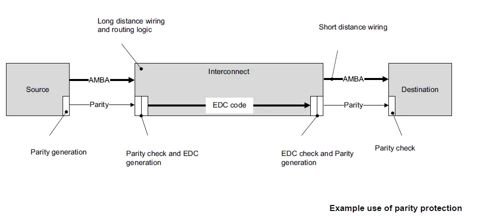
The image shows one example of where parity protection can be used.
- The Source generates parity for the outgoing AMBA interface signals.
- At the Interconnect input, parity is checked. The Interconnect can then generate its internal EDC code for long-distance wiring and routing logic.
- At the Interconnect output, the EDC is checked and parity is generated again for the outgoing AMBA interface.
- The Destination receives the AMBA signals and parity signals, then checks parity at its input.
The key idea is that parity protects the interface between components, while an internal EDC scheme can protect logic and longer wiring inside a component such as an interconnect.
Check_Type configuration
The EDC scheme of the APB interface is defined by the Check_Type property.
| Check_Type value | Meaning |
|---|---|
| False | There are no checking signals on the interface. |
| Odd_Parity_Byte_All | Odd parity checking is included for all signals. Each bit of the parity signal covers up to 8 bits. |
If Check_Type is not declared, it is considered to be False. Check signaling can be added to APB5 interfaces only.
Odd parity rule
Odd parity means there is always an odd number of asserted bits across the interface signal and its check signal. Check signals are associated with each interface signal.
Common rules for byte parity interface protection:
- Each check bit covers no more than 8 payload bits.
- For a check signal wider than 1 bit, check bit n corresponds to payload bits [(8n+7):8n].
- If the payload is not an integer number of bytes, the most significant check bit covers fewer than 8 bits in the most significant portion of the payload.
- Parity signals that cover critical control signals are defined with a single parity bit. The single odd parity bit is the inversion of the original critical control signal.
- Check signals must be driven correctly in every cycle where the Check Enable term is true.
- Parity signals must be driven for all bits in the associated payload, whether or not those bits are actively used in the transfer.
- If some signals covered by a check signal are not present, the missing signals are assumed to be LOW.
- If none of the signals covered by a check signal are present, the check signal is omitted from the interface.
Error detection behavior
The APB specification defines the parity signaling, but it does not prescribe exactly how a component or system must react after detecting a parity error. The effect of a flipped bit depends on the system and affected signals.
When an error is detected, the Completer can:
- Terminate or propagate the transfer.
- Correct the parity check signal or propagate the error.
- Update its memory or leave it untouched.
- Signal an error response through other means, for example with an interrupt.
Parity check signals
Check signals are synchronous to PCLK and must be driven correctly every cycle in which the Check Enable term is true.
| Check signal | Signals covered | Width | Check Enable |
|---|---|---|---|
| PADDRCHK | PADDR | ceil(ADDR_WIDTH/8) | PSEL |
| PCTRLCHK | PPROT, PWRITE, PNSE | 1 | PSEL |
| PSELxCHK | PSELx | 1 | PRESETn |
| PENABLECHK | PENABLE | 1 | PSEL |
| PWDATACHK | PWDATA | DATA_WIDTH/8 | PSEL && PWRITE |
| PSTRBCHK | PSTRB | 1 | PSEL && PWRITE |
| PREADYCHK | PREADY | 1 | PSEL && PENABLE |
| PRDATACHK | PRDATA | DATA_WIDTH/8 | PSEL && PENABLE && PREADY && !PWRITE |
| PSLVERRCHK | PSLVERR | 1 | PSEL && PENABLE && PREADY |
| PWAKEUPCHK | PWAKEUP | 1 | PRESETn |
| PAUSERCHK | PAUSER | ceil(USER_REQ_WIDTH/8) | PSEL |
| PWUSERCHK | PWUSER | ceil(USER_DATA_WIDTH/8) | PSEL && PWRITE |
| PRUSERCHK | PRUSER | ceil(USER_DATA_WIDTH/8) | PSEL && PENABLE && PREADY && !PWRITE |
| PBUSERCHK | PBUSER | ceil(USER_RESP_WIDTH/8) | PSEL && PENABLE && PREADY |
APB Protocol