Tutorials
Protocols
Learn More
Switch Level Modeling
The switch level modeling is used to model digital circuits at the MOS level transistor. In this era, digital circuits have become more complex and involve millions of transistors, so modeling at the transistor level is rarely used by the designer. Hence, mostly higher abstraction levels are used for design description.
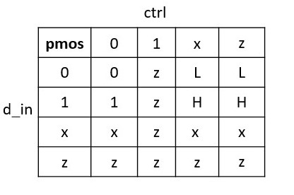
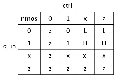
NMOS and PMOS switches
The keywords ‘nmos’ and ‘pmos’ are used to model NMOS and PMOS respectively.
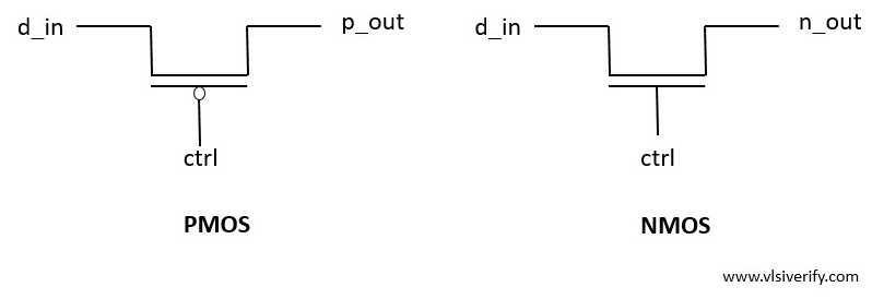
Example:
module switch_modeling (
  input d_in, ctrl,
  output p_out, n_out);

  pmos p1(p_out, d_in, ctrl);
  nmos n1(n_out, d_in, ctrl);

endmodule
Output:
At time = 0: ctrl = 0, d_in = 0, p_out = 0, n_out = z
At time = 5: ctrl = 1, d_in = 0, p_out = z, n_out = 0
At time = 10: ctrl = 1, d_in = 1, p_out = z, n_out = 1
At time = 15: ctrl = 0, d_in = 1, p_out = 1, n_out = z
At time = 20: ctrl = 0, d_in = 0, p_out = 0, n_out = z
CMOS switch
A CMOS is modeled with a combination of NMOS and PMOS devices.
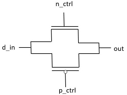
cmos
module cmos_modeling (
  input d_in, p_ctrl, n_ctrl,
  output out);

  cmos p1(out, d_in, p_ctrl, n_ctrl);

endmodule
output:
At time = 0: d_in = 0, p_ctrl = 0, n_ctrl = 0, out = 0
At time = 5: d_in = 0, p_ctrl = 1, n_ctrl = 0, out = 0
At time = 10: d_in = 1, p_ctrl = 1, n_ctrl = 0, out = 1
At time = 15: d_in = 0, p_ctrl = 1, n_ctrl = 0, out = 0
At time = 20: d_in = 0, p_ctrl = 1, n_ctrl = 1, out = 0
At time = 25: d_in = 1, p_ctrl = 1, n_ctrl = 1, out = 1
At time = 30: d_in = 0, p_ctrl = 1, n_ctrl = 1, out = 0
Power and ground
The power (Vcc) and ground (GND) sources need to be defined in transistor level modeling to provide the supply to the signals.
Keywords used: supply1(Vcc) and supply0 (GND)
module power_modeling (
  output vcc, gnd
);

  supply1 high;
  supply0 low;

  assign vcc = high;
  assign gnd = low;
endmodule
Output:
At time = 0: vcc = 1, gnd = 0Bidirectional switches
As of now, we have discussed unidirectional switches like PMOS, NMOS, and CMOS that conduct from drain to source. Sometimes in the design, there is a need to have a bi-directional switch that can be driven from any of the device sides.
Keywords used: tran, tranif0, and tranif1
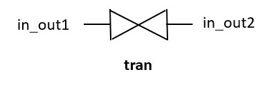
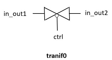
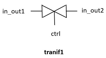
All tran, tranif0, and tranif1 behaves as a buffer from in either of the device side,
|
Switch types |
Description |
|
tran |
Connects in_out1 and in_out2 |
|
tranif0 |
Connects in_out1 and in_out2 if control signal is 0. If the control signal is 1, then
|
|
tranif1 |
Connects in_out1 and in_out2 if control signal is 1. If the control signal is 0, then
|
module bidirectional_modeling (
  input in_out1, ctrl,
  output in_out2, in_out2_if0, in_out2_if1);

  tran t1(in_out1, in_out2);
  tranif0 t2(in_out1, in_out2_if0, ctrl);
  tranif1 t3(in_out1, in_out2_if1, ctrl);
endmodule
Output:
At time = 0: ctrl = 0, in_out1 = 0, in_out2 = 0, in_out2_if0 = 0, in_out2_if1 = z
At time = 5: ctrl = 0, in_out1 = 1, in_out2 = 1, in_out2_if0 = 1, in_out2_if1 = z
At time = 10: ctrl = 1, in_out1 = 1, in_out2 = 1, in_out2_if0 = z, in_out2_if1 = 1
At time = 15: ctrl = 1, in_out1 = 0, in_out2 = 0, in_out2_if0 = z, in_out2_if1 = 0
Resistive switches
The resistive switches provide a high impedance from source to drain with a reduction in signal strength as compared to regular switches. All PMOS, NMOS, CMOS, and bidirectional switches can be modeled as resistive devices.
Keyword used: ‘r’ as a prefix to the regular switches.
|
Resistive switches |
Resistive keywords |
|
Resistive pmos |
rpmos |
|
Resistive nmos |
rnmos |
|
Resistive cmos |
rcmos |
|
Resistive tran |
rtran |
|
Resistive tranif0 |
rtranif0 |
|
Resistive tranif1 |
rtranif1 |
module resistive_modeling (
  input in_out1, ctrl,
  output in_out2, in_out2_if0, in_out2_if1);

  rtran t1(in_out1, in_out2);
  rtranif0 t2(in_out1, in_out2_if0, ctrl);
  rtranif1 t3(in_out1, in_out2_if1, ctrl);
endmodule
Output:
At time = 0: ctrl = 0, in_out1 = 0, in_out2 = 0, in_out2_if0 = 0, in_out2_if1 = z
At time = 5: ctrl = 0, in_out1 = 1, in_out2 = 1, in_out2_if0 = 1, in_out2_if1 = z
At time = 10: ctrl = 1, in_out1 = 1, in_out2 = 1, in_out2_if0 = z, in_out2_if1 = 1
At time = 15: ctrl = 1, in_out1 = 0, in_out2 = 0, in_out2_if0 = z, in_out2_if1 = 0
Verilog Tutorials